
The industry is moving toward Advanced IC Packaging—where chips are becoming more compact, complex, and performance-intensive than ever before.
𝐓𝐡𝐞 𝐂𝐡𝐚𝐥𝐥𝐞𝐧𝐠𝐞: 𝐒𝐞𝐞𝐢𝐧𝐠 𝐭𝐡𝐞 𝐔𝐧𝐬𝐞𝐞𝐧 
With advanced multi-layered structures and high-density interconnects, internal defects are no longer visible to the naked eye or conventional inspection methods. Hidden killers like solder voids, micro-cracks, and internal delamination can compromise the reliability of next-gen tech if left undetected.
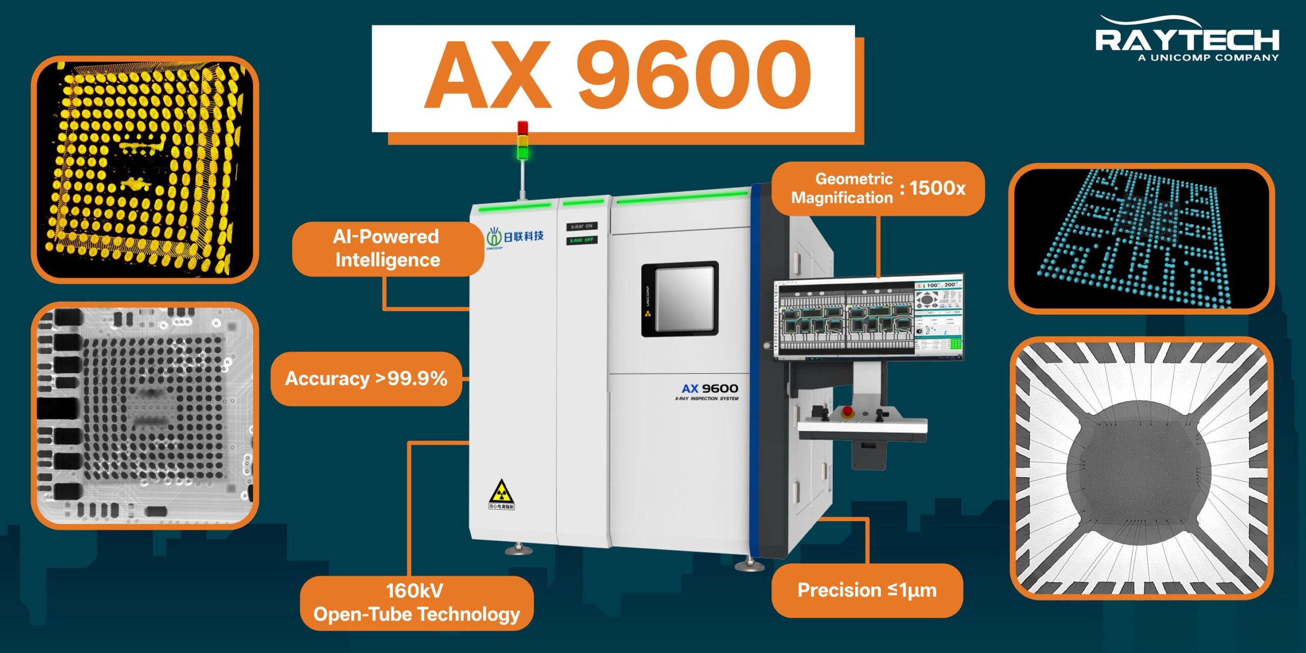
In this new era, quality assurance isn’t just a final step; it’s a core competitive advantage. Let’s introduce Unicomp’s Industrial AI-powered inspection equipment, AX9600 to you.
Key Technical Specs:
• 160kV Open-Tube Technology: Penetrate dense materials with ease.
• 1μm Focal Spot Resolution: Detect even the most minute anomalies in TSV structures and wafer bump interconnects.
• Up to 1500X Geometric Magnification: Crystal-clear visualization of internal architectures.
𝐒𝐞𝐜𝐮𝐫𝐢𝐧𝐠 𝐌𝐚𝐥𝐚𝐲𝐬𝐢𝐚’𝐬 𝐒𝐩𝐨𝐭 𝐨𝐧 𝐭𝐡𝐞 𝐆𝐥𝐨𝐛𝐚𝐥 𝐒𝐭𝐚𝐠𝐞
As Malaysia evolves into a higher-value semiconductor hub, integrating advanced inspection solutions like the AX9600 ensures our local manufacturing remains precise, reliable, and globally competitive.
We aren’t just part of the supply chain; we are enabling the high-performance chip architectures of tomorrow.